APPLICATIONS
| Market | Application | Related Product | Features | ||
|---|---|---|---|---|---|
| Probe Technology | KI Model | ||||
| Memory Test | NAND Flash | High Density Memory | MEMS | Cygnus |
Full Wafer Contact for 12" Wafer Up to 2,000 DUT / 62,000 Pins Utilizing MEMS Probes 1.2A C.C.C. -40℃ ~ 125℃ Operating Temp. |
| DRAM / HBM | Ultra High Density Memory | MEMS | Orion |
Full Wafer Contact for 12" Wafer Up to 2,500 DUT/ 150,000 Pins Utilizing MEMS Probes 1.0A C.C.C. -40℃ ~ 105℃ Operating Temp |
|
| Logic Test | SoC | Fine-Pitch Logic Device (AP, CPU, GPU, ASIC, FPGA, MCU, Connectivity) |
MEMS Vertical | Taurus |
MEMS Probe Min. 70㎛ Pitch Full array Up to 8 DUT / 50,000 Pins+ C.C.C. : > 0.8~2.5 A Probe Force can be customized Space Transformer (MLC, MLO, Cu wire) utilized |
| CIS | High performance Imaging | MEMS CIS | Sirius |
Up to 64 DUT+ Image Test All DUT Characteristic Uniformity Min. 60㎛ Pad Pitch >20 Gbps Short Scrub mark |
|
| DDI, MCU, Smart Card | Conventional & Cost-effective | Cantilever-Needle | Cantilever |
Pitch : Fine pitch & Multi-DUT Min. Pitch : DDI ( 12.5/25μm, 23μm) SoC (50μm) Min. Pad Size : DDI (13X30μm) SoC (40X40μm) Test Temp : -25℃ ~ 125℃ |
|
| DC Parametric | Wafer level leakage DC Test | MEMS / Cantilever | DC Para |
Min. 60um pad pitch Low leakage DC Test (Under 500fA leakage) -20~125 ℃ Operating Temp. Easy Repair Small pad contact (Pad size: 35um x 35um) |
|
Application & KI Product Example
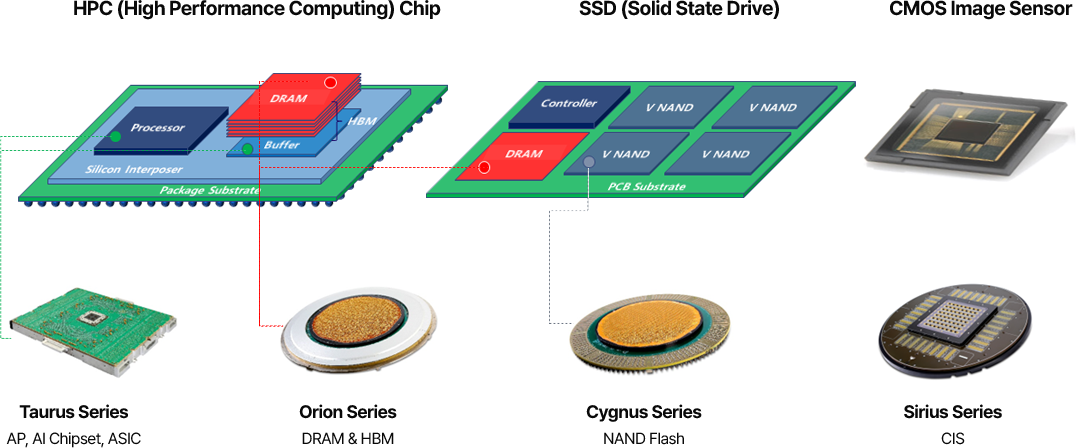
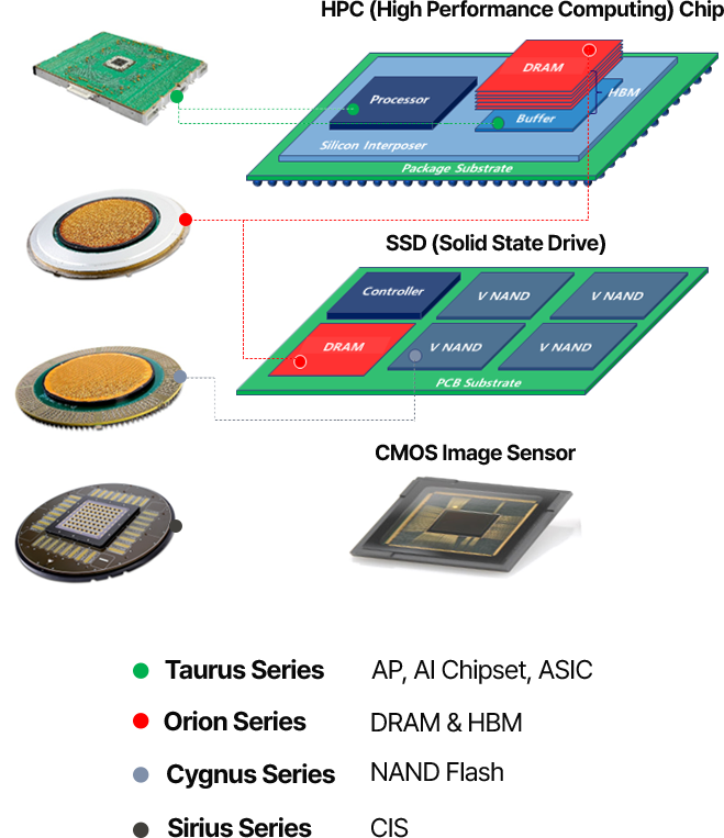
Memory
The rapid proliferation of memory devices and the exponential growth of data are driving strong demand for DRAM and Flash memory. As memory IC technologies continue to scale and diversify, semiconductor manufacturers face significant challenges such as high-parallelism testing and full-wafer contact requirements.KI’s high-performance wafer test solutions enable chip makers to optimize yield, reduce overall test costs, and accelerate time-to-market for next-generation memory devices.
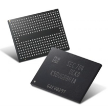
NAND FLASH
AI, HPC, and the growth of consumer electronics are advancing next-generation NAND Flash memory for Small form factor, high density, high speed.
KI’s wafer probe cards offer cost-effective solutions for NAND memory test.
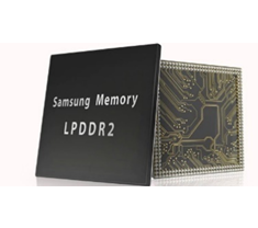
DRAM & HBM
The DRAM nodes continue to shrink and die count per wafer is increasing, driven by the needs to increase bit density and reduce memory device cost.
KI is keeping pace with this advancement of DRAM technologies.
Logic
The semiconductor technology is facing a big evolving challenges, by the development of artificial intelligence (AI), high-performance computing (HPC), automotive technology, and mobile devices. As devices become smaller, more powerful, and interconnected, the demand for probe pin's fine pitch, high current carrying capacity and mechanical durability for reliable test solutions is greater than ever. To address these challenges, KI's logic wafer probe cards are designed to provide the precision and efficiency needed for next-generation semiconductor testing.
System on Chip (SoC)
AI, HPC, and the growth of consumer electronics are advancing next-generation logic technologies.
KI’s wafer probe cards deliver precision and efficiency to meet the evolving test challenges.
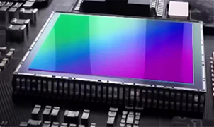
CMOS Image Sensor (CIS)
An image sensor converts light energy into electrical energy to create images, and serves a function similar to the film in a camera.
KI's optical probe cards offer customized solutions for testing CMOS image sensors.
Display Driver IC (DDI)
Display Driver IC is an indispensable semiconductor chip to operate each sub-pixels. DDI accepts a signal of an image from the CPU of the device and generates and controls the output signals.