Memory
NAND FLASH
As the use of AI (artificial intelligence) expands, demand for next-generation memory products is increasing in data centers and AI servers. Next-generation memory products feature high capacity, high-speed computation, high performance, and low power consumption.
FLASH memory can retain data regardless of power on/off and is applied to USBs, SD cards, SSDs, etc.
The number of layers in 3D NAND is expected to increase from the current 200-300 layers to 500-600 layers within the next few years. Consequently, hybrid bonding technology is anticipated to be applied and expanded in 3D NAND, similar to DRAM. This brings challenges such as cell current management, new equipment process development, stress/warpage compensation processes, defect-free hybrid bonding technology, and XY cell miniaturization.
KI is collaborating with the world's leading chipmakers to develop solutions for the increasing number of chip I/Os, driven by the trend toward higher integration and faster speeds in NAND Flash chips.
DRAM & HBM
As AI adoption accelerates, demand for next-generation memory products in data centers and AI servers continues to grow. These advanced memory solutions require higher capacity, faster computational performance, improved efficiency, and lower power consumption.
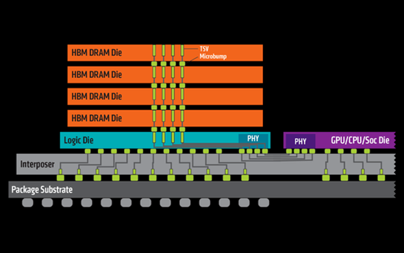
High Bandwidth Memory (HBM) is a key technology that vertically stacks multiple DRAM chips and interconnects them through Through-Silicon Vias (TSVs) to dramatically increase data-processing bandwidth. Traditionally, HBM has been manufactured using a thermal compression (TC) bonding method, which relies on inserting fine micro-bumps between DRAM dies. However, as the number of stacked layers expands to 16 or even 20, this TC-based approach faces growing technical constraints. Within the limited HBM package height (maximum 775 µm), thinning each DRAM die or reducing die-to-die spacing provides only marginal relief.
To overcome these limitations, DRAM manufacturers have been developing hybrid bonding technology, in which copper-to-copper interconnections are formed directly between chips or wafers. By eliminating micro-bumps, hybrid bonding can significantly reduce HBM package thickness, while simultaneously enabling higher I/O density and better thermal dissipation—both essential for next-generation AI workloads.
KI is closely aligned with these technological trends and is actively collaborating with customers from the early development stage to support the rapid transition toward hybrid-bonding-based HBM solutions.