News
[News Article] A Challenge for Sustainable Growth: Korea Instrument Global Probe Card Strategy
Name KI
Date 2025-10-23
Hit 1493
https://www.theworldfolio.com/interviews/A-Challenge-for-Sustainable-Growth-Korea-Instrument-s-Global-Probe-Card-Strategy/7073/
A Challenge for Sustainable Growth: Korea Instrument's Global Probe Card Strategy
Interview - October 21, 2025
Korea Instrument's semiconductor probe cards enhance NAND, DRAM and HBM wafer testing effectiveness, supporting Korea global dominance in memory chips. Today, Korea Instrument uses its long-standing expertise to diversify offerings and advance semiconductor testing.
OH SUNG-TAK, CEO OF KOREA INSTRUMENTSHARE


OH SUNG-TAK | CEO OF KOREA INSTRUMENT
Over the years, Korea Instrument has collaborated closely with Korean Chipmaker and OSAT. Given Korea’s industrial structure and growing competitiveness, do you believe now is an opportune moment for the Korean semiconductor ecosystem to diversify its portfolio and expand into more globalized systems?
Yes, but I don't want to say it is an opportune moment. I think this is a challenge that needs to be done for sustainable growth and survival. Major Korean semiconductor companies such as Samsung and SK Hynix have firmly established themselves and achieved remarkable growth. However, for SMEs in Korea, internationalization and diversification are essential for survival and growth. By leveraging our long-standing expertise and partnerships, I think now is the right time to diversify globally and strengthen our competitiveness. This is not just a challenge, but also a window of opportunity for us to expand into new international markets.
In that context, what opportunities do you foresee for Korea Instrument, particularly in areas like probe cards, which are crucial for semiconductor testing?
Our primary business revolves around probe cards, which are indispensable in semiconductor manufacturing. Demand for these products will continue to grow. For example, as High Bandwidth Memory (HBM) adoption expands, the demand for probe cards will rise accordingly. We project steady growth in this segment through at least 2030, roughly a decade of sustained expansion.
To prepare for the long-term growth of the memory market driven by AI trends, we have initiated development work on DRAM-related products, and earlier this year, Samsung approved our new probe card for both DRAM and HBM as well. Collectively, these developments point to significant opportunities in the coming years.
At present, only a few global and Korean companies supply probe cards for HBM. This scarcity means growth potential is substantial. By 2030, we expect to see industry-wide growth rates of up to 10%. We intend to seize this opportunity by broadening our product portfolio, supplying DRAM and HBM probe cards to Samsung this year, high-end DRAM and HBM probe cards next year, and gradually expanding into even more advanced solutions.
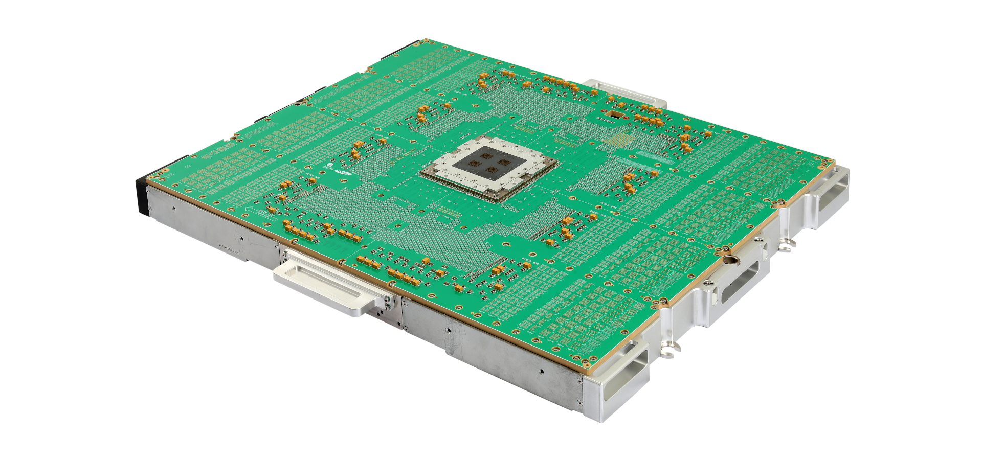
Korea Instrument's Headquarter
Beyond memory, you also mentioned the potential in LSI (Large-Scale Integration) markets. How does Korea Instrument intend to participate?
The total probe card market size is estimated between $2.5B and $3B. Within this, the Logic market is estimated at $1.2B to $1.5B, similar to the Memory market, and is expected to grow by more than 7% annually through 2030, driven primarily by AI and automotive applications.
Until now, we have been supplying Logic products to Samsung in the SoC and CIS sectors, as well as to OSAT companies in the Cantilever and DDI (Display Driver IC) segments, but we have faced limitations in expanding our market share. As a result, based on technology verified at Samsung LSI, we have developed probe pins with differential characteristics, such as long lifespan and high current-carrying capacity (CCC), to actively participate in the emerging VPC global market.
In addition, to expand our reach to global Fabless, Foundry, and OSAT customers, we plan to conduct overseas marketing activities aimed at establishing international customer service bases and sales networks.
Could you clarify the differences between logic chips and NAND memory, particularly in terms of challenges for probe card suppliers?
In general, logic and NAND memory chips require the development of probe cards with ultra-fine pitches and extreme precision to keep pace with technological evolution, which optimizes yields in the testing process, reduces overall test costs, shortens the time-to-market for advanced chips, and enables high integration. A specific technical challenge common to probe cards is maintaining current-carrying capacity (CCC) and mechanical durability as the pins become thinner.
The differences between logic chips and NAND memory chips in terms of probe card technology are as follows. Memory chip probe cards face the technical challenge of performing full-wafer contact tests with an increased number of DUTs (Devices Under Test) per wafer, requiring high parallelism through probe pins that satisfy both fine pitch and high precision.
On the other hand, logic chips, such as APs and CPUs, have much higher IO integration than memory chips relative to the number of channels available between probe cards and testers. Therefore, it is not feasible to increase the DUT count at the wafer test stage to the same level as memory probe cards.
Because a low DUT count requires multiple shots per wafer for inspection, the durability and precision of the probe pins must be further enhanced. Vertical-type probe pins are applied to handle finer pitches than those used in memory chips. Through the design of MEMS probe pins and the development of new materials, we have expanded business opportunities by demonstrating our technological capabilities in addressing these challenges. KI's Long Life, High CCC VPC products, which I mentioned earlier, are expected to perform well in the market, as they effectively address these technical challenges.
With AI, 5G, IoT, and automotive sectors driving semiconductor demand, how do you assess long- and short-term growth opportunities across these fields?
Artificial Intelligence is undoubtedly the strongest growth driver. As AI workloads expand, demand in the server and data center markets will increase dramatically. In contrast, the mobile phone sector faces limitations unless new breakthrough technologies emerge.
From a mid- to long-term perspective, I believe servers and data centers will be the most dynamic growth segments. These applications require cutting-edge semiconductors produced at 2nm and below, often with complex 3D architectures. This creates both economic and technical challenges for testing. As requirements become more exacting, probe cards must evolve to match.
At Korea Instrument, we are already preparing next-generation probe cards capable of supporting these fine processes, including DDR5 for servers and LPDDR for mobile applications. By the end of this year, we aim to deliver DRAM probe cards to customers, and from next year, expand into HBM.
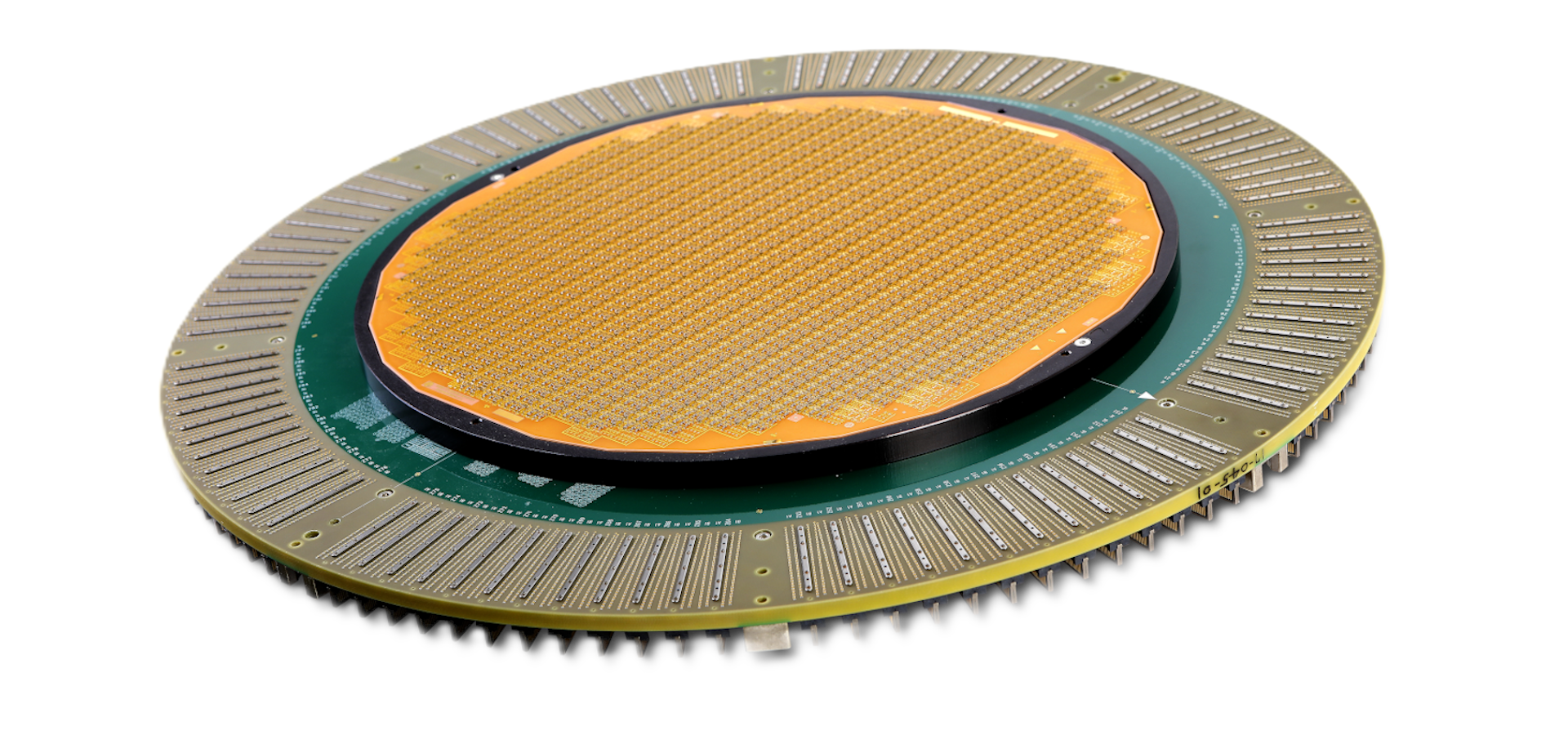
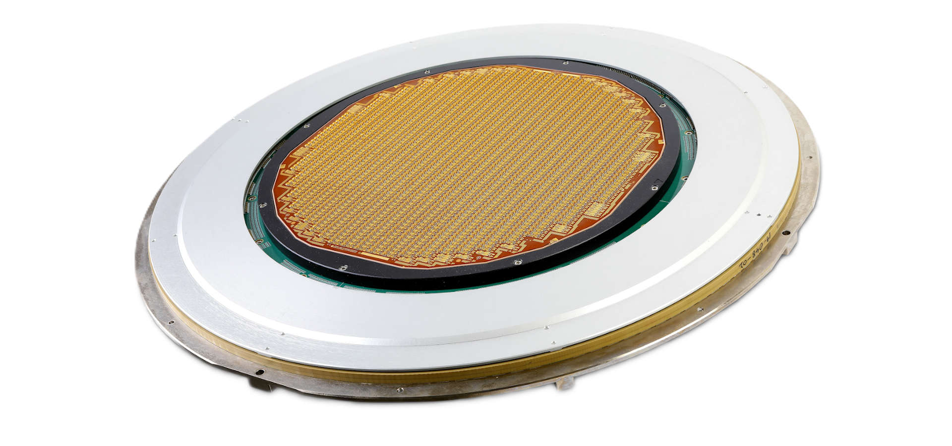 DRAM and HBM MEMS Probe Cards
PreviousNext
Korea Instrument has been a long-standing partner of Samsung. What differentiates your company from competitors in probe card manufacturing?
Our biggest strength is our end-to-end integration. From the initial design stage through simulation, production, fabrication, and final assembly, we manage the entire process internally. This allows us to respond quickly and precisely to customer’s requirements.
We also develop customized equipment exclusively for our use, ensuring we maintain technical independence and efficiency. Our simulation and electrical design capabilities, particularly in signal integrity and power performance, give us a one-to-two-year competitive lead over peers.
Ultimately, what sets us apart is our ability to collaborate closely with clients from conception to delivery, providing consistency, speed, and tailored solutions that others struggle to match.
How does Korea Instrument approach collaboration with global equipment suppliers across Japan or the U.S.?
Collaboration is essential. In bonding equipment, technologies like fine pitch movement, laser power, and precision control must be integrated with probe card design. Without close cooperation, equipment cannot deliver full performance.
From a perspective of test performance verification, currently, we are co-developing high-speed probe cards with one of global test maker, particularly for logic chip test. This kind of joint development is a model we intend to expand, not only with this company but also with other Japanese and American partners when opportunities arise.
In memory, collaboration tends to be more predetermined with Samsung. But in LSI, because requirements are more specialized, joint development with equipment makers is both possible and necessary.
Finally, what is your long-term vision for Korea Instrument?
My vision is for Korea Instrument to become a truly global player in the probe card market. Within the next three to five years, we aim to move beyond our domestic leadership position and establish ourselves as a top-tier supplier in the global probe card market.
We are already making progress: this year we entered DRAM and HBM supply, and in parallel we are preparing for expansion into the LSI sector, particularly in Taiwan and China. DRAM and LSI together will significantly expand our market share.
Diversifying across both memory and LSI not only spreads risk but also strengthens our resilience. I believe this dual strategy is the right approach to ensure stability and long-term growth. Korea Instrument has the history, the technical foundation, and now the strategic ambition to play a central role in the global semiconductor ecosystem.
For more details, explore their website at https://www.kicl.co.kr/
隐私政策
韩国仪器(株)(以下简称“公司”)为了保护信息主体的个人信息,并根据《个人信息保护法》第30条迅速顺畅地处理相关投诉,制定并公开如下个人信息处理指南。
第1条 个人信息处理目的
“公司”出于以下目的处理个人信息。所处理的个人信息不会用于以下目的以外的其他用途,若利用目的发生变更,将根据《个人信息保护法》第18条采取获得单独同意等必要措施。
A. “咨询”相关的咨询及答复
出于处理客户咨询、投资咨询、人才招聘咨询等目的处理个人信息。
第2条 处理的个人信息项目
“公司”在提供服务所需的最小范围内收集并利用个人信息。
A. 无需信息主体同意即可处理的个人信息项目
在互联网服务使用过程中,可能会自动生成并收集以下个人信息项目。
- IP地址、Cookie、MAC地址、服务使用记录、访问记录、不良使用记录等
B. 经信息主体同意处理的个人信息项目
“公司”根据《个人信息保护法》第15条第1款第1项及第22条第1款第7项,在获得信息主体同意后处理以下个人信息项目。
- 客户支持咨询:收集项目:姓名、电子邮件、联系方式
第3条 个人信息的处理及保存期限
“公司”在法令规定的个人信息保存·利用期限或收集个人信息时获得信息主体同意的个人信息保存·利用期限内处理并保存个人信息。
各项个人信息的处理及保存期限如下:
客户支持咨询:永久(收到删除请求时立即删除)
但是,若符合以下事由,则保留至该事由结束为止:
因违反相关法令正在进行调查、侦查的情况:至该调查、侦查结束为止
因使用网站而残留债权、债务关系的情况:至相关债权、债务关系结算完毕为止
第4条 个人信息的销毁程序及方法
个人信息在保存期限届满、处理目的达成等个人信息变得不再必要时,将延迟销毁相关个人信息。
尽管从信息主体处获得的个人信息保存期限已过或处理目的已达成,但根据其他法令仍需继续保存个人信息时,将该个人信息(或个人信息文件)转移到单独的数据库(DB)或更改存放场所进行保存。
个人信息销毁的程序及方法如下:
销毁程序
“公司”针对需销毁的个人信息(或个人信息文件)制定销毁计划并进行销毁。“公司”选定发生销毁理由的个人信息(或个人信息文件),经公司个人信息保护负责人的批准后销毁个人信息(或个人信息文件)。
销毁方法
“公司”对以电子文件形式记录、存储的个人信息,采用低级格式化(Low Level Format)等方法使其无法恢复记录;对记录、存储在纸质文档上的个人信息,则使用碎纸机粉碎或通过焚烧销毁。
第5条 个人信息安全性确保措施
“公司”为了确保个人信息的安全性,正在采取以下措施:
管理措施: 制定及实施内部管理计划、定期员工培训
技术措施: 个人信息处理系统等的访问权限管理、安装访问控制系统、安装及更新安全程序
第6条 关于自动个人信息收集装置的安装、运营及拒绝的事项
< 自动个人信息收集装置安装及运营 > “公司”为了向用户提供个性化的定制服务,会使用存储并随时调用使用信息的“Cookie”。
Cookie是运营网站的服务器(http)向用户电脑浏览器发送的少量信息,有时也会存储在用户PC电脑的硬盘中。
信息主体可以通过Web浏览器选项设置来允许或阻止Cookie。但是,如果拒绝存储Cookie,可能会在使用定制服务时遇到困难。
Web浏览器中的允许/阻止Cookie设置
- Chrome: 浏览器设置 > 隐私和安全 > 清除浏览数据
- Edge: 浏览器设置 > Cookie 和网站权限 > 管理和删除 Cookie 及网站数据
移动浏览器中的允许/阻止Cookie设置
- Chrome: 移动浏览器设置 > 隐私和安全 > 清除浏览数据
- Safari: 移动设备设置 > Safari > 高级 > 阻止所有 Cookie
- Samsung Internet: 移动浏览器设置 > 浏览历史 > 清除浏览数据
第7条 个人信息保护负责人
“公司”全面负责个人信息处理业务,为处理与个人信息处理相关的信息主体投诉及损失救济等,指定个人信息保护负责人如下:
▶ 个人信息保护担当部门
部门名称: 人事团队 (HR Team)
联系方式: +82-31-375-5900
Email: ki.hr@kicl.co.kr
信息主体在利用“公司”的服务(或业务)过程中发生的所有个人信息保护相关咨询、投诉处理、损失救济等事项,均可咨询个人信息保护负责人及担当部门。“公司”将对信息主体的咨询及时给予答复和处理。
第8条 个人信息处理方针变更
本个人信息处理方针自2025年09월 01日起施行。