News
[News Article] A Challenge for Sustainable Growth: Korea Instrument Global Probe Card Strategy
Name KI
Date 2025-10-23
Hit 1492
https://www.theworldfolio.com/interviews/A-Challenge-for-Sustainable-Growth-Korea-Instrument-s-Global-Probe-Card-Strategy/7073/
A Challenge for Sustainable Growth: Korea Instrument's Global Probe Card Strategy
Interview - October 21, 2025
Korea Instrument's semiconductor probe cards enhance NAND, DRAM and HBM wafer testing effectiveness, supporting Korea global dominance in memory chips. Today, Korea Instrument uses its long-standing expertise to diversify offerings and advance semiconductor testing.
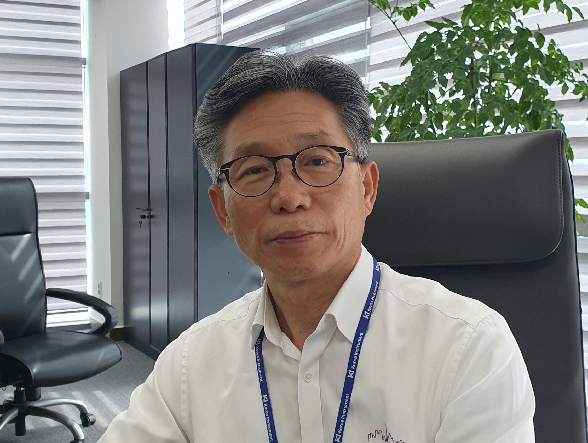
OH SUNG-TAK, CEO OF KOREA INSTRUMENTSHARE


OH SUNG-TAK | CEO OF KOREA INSTRUMENT
Over the years, Korea Instrument has collaborated closely with Korean Chipmaker and OSAT. Given Korea’s industrial structure and growing competitiveness, do you believe now is an opportune moment for the Korean semiconductor ecosystem to diversify its portfolio and expand into more globalized systems?
Yes, but I don't want to say it is an opportune moment. I think this is a challenge that needs to be done for sustainable growth and survival. Major Korean semiconductor companies such as Samsung and SK Hynix have firmly established themselves and achieved remarkable growth. However, for SMEs in Korea, internationalization and diversification are essential for survival and growth. By leveraging our long-standing expertise and partnerships, I think now is the right time to diversify globally and strengthen our competitiveness. This is not just a challenge, but also a window of opportunity for us to expand into new international markets.
In that context, what opportunities do you foresee for Korea Instrument, particularly in areas like probe cards, which are crucial for semiconductor testing?
Our primary business revolves around probe cards, which are indispensable in semiconductor manufacturing. Demand for these products will continue to grow. For example, as High Bandwidth Memory (HBM) adoption expands, the demand for probe cards will rise accordingly. We project steady growth in this segment through at least 2030, roughly a decade of sustained expansion.
To prepare for the long-term growth of the memory market driven by AI trends, we have initiated development work on DRAM-related products, and earlier this year, Samsung approved our new probe card for both DRAM and HBM as well. Collectively, these developments point to significant opportunities in the coming years.
At present, only a few global and Korean companies supply probe cards for HBM. This scarcity means growth potential is substantial. By 2030, we expect to see industry-wide growth rates of up to 10%. We intend to seize this opportunity by broadening our product portfolio, supplying DRAM and HBM probe cards to Samsung this year, high-end DRAM and HBM probe cards next year, and gradually expanding into even more advanced solutions.
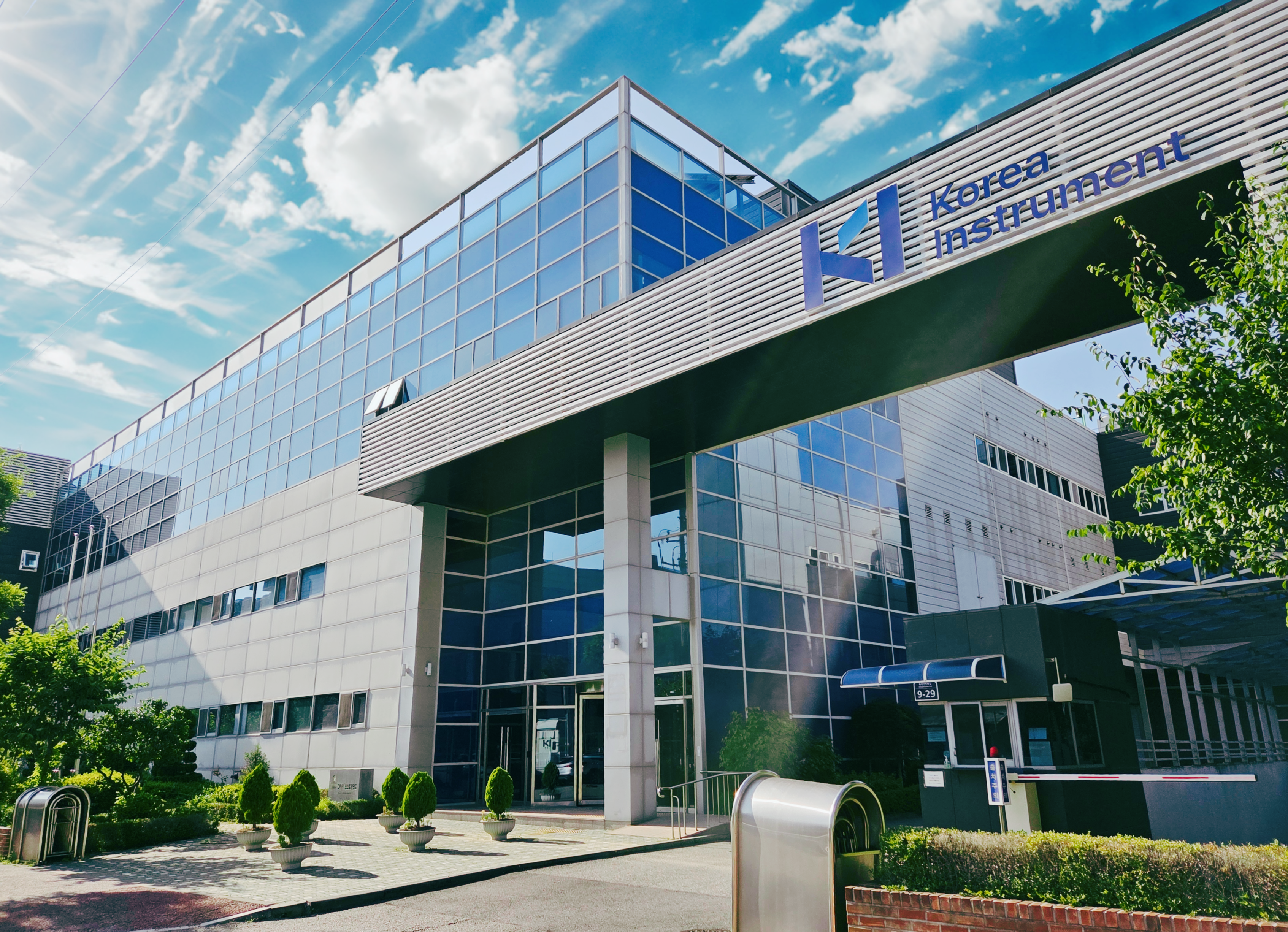
Korea Instrument's Headquarter
Beyond memory, you also mentioned the potential in LSI (Large-Scale Integration) markets. How does Korea Instrument intend to participate?
The total probe card market size is estimated between $2.5B and $3B. Within this, the Logic market is estimated at $1.2B to $1.5B, similar to the Memory market, and is expected to grow by more than 7% annually through 2030, driven primarily by AI and automotive applications.
Until now, we have been supplying Logic products to Samsung in the SoC and CIS sectors, as well as to OSAT companies in the Cantilever and DDI (Display Driver IC) segments, but we have faced limitations in expanding our market share. As a result, based on technology verified at Samsung LSI, we have developed probe pins with differential characteristics, such as long lifespan and high current-carrying capacity (CCC), to actively participate in the emerging VPC global market.
In addition, to expand our reach to global Fabless, Foundry, and OSAT customers, we plan to conduct overseas marketing activities aimed at establishing international customer service bases and sales networks.
Could you clarify the differences between logic chips and NAND memory, particularly in terms of challenges for probe card suppliers?
In general, logic and NAND memory chips require the development of probe cards with ultra-fine pitches and extreme precision to keep pace with technological evolution, which optimizes yields in the testing process, reduces overall test costs, shortens the time-to-market for advanced chips, and enables high integration. A specific technical challenge common to probe cards is maintaining current-carrying capacity (CCC) and mechanical durability as the pins become thinner.
The differences between logic chips and NAND memory chips in terms of probe card technology are as follows. Memory chip probe cards face the technical challenge of performing full-wafer contact tests with an increased number of DUTs (Devices Under Test) per wafer, requiring high parallelism through probe pins that satisfy both fine pitch and high precision.
On the other hand, logic chips, such as APs and CPUs, have much higher IO integration than memory chips relative to the number of channels available between probe cards and testers. Therefore, it is not feasible to increase the DUT count at the wafer test stage to the same level as memory probe cards.
Because a low DUT count requires multiple shots per wafer for inspection, the durability and precision of the probe pins must be further enhanced. Vertical-type probe pins are applied to handle finer pitches than those used in memory chips. Through the design of MEMS probe pins and the development of new materials, we have expanded business opportunities by demonstrating our technological capabilities in addressing these challenges. KI's Long Life, High CCC VPC products, which I mentioned earlier, are expected to perform well in the market, as they effectively address these technical challenges.
With AI, 5G, IoT, and automotive sectors driving semiconductor demand, how do you assess long- and short-term growth opportunities across these fields?
Artificial Intelligence is undoubtedly the strongest growth driver. As AI workloads expand, demand in the server and data center markets will increase dramatically. In contrast, the mobile phone sector faces limitations unless new breakthrough technologies emerge.
From a mid- to long-term perspective, I believe servers and data centers will be the most dynamic growth segments. These applications require cutting-edge semiconductors produced at 2nm and below, often with complex 3D architectures. This creates both economic and technical challenges for testing. As requirements become more exacting, probe cards must evolve to match.
At Korea Instrument, we are already preparing next-generation probe cards capable of supporting these fine processes, including DDR5 for servers and LPDDR for mobile applications. By the end of this year, we aim to deliver DRAM probe cards to customers, and from next year, expand into HBM.
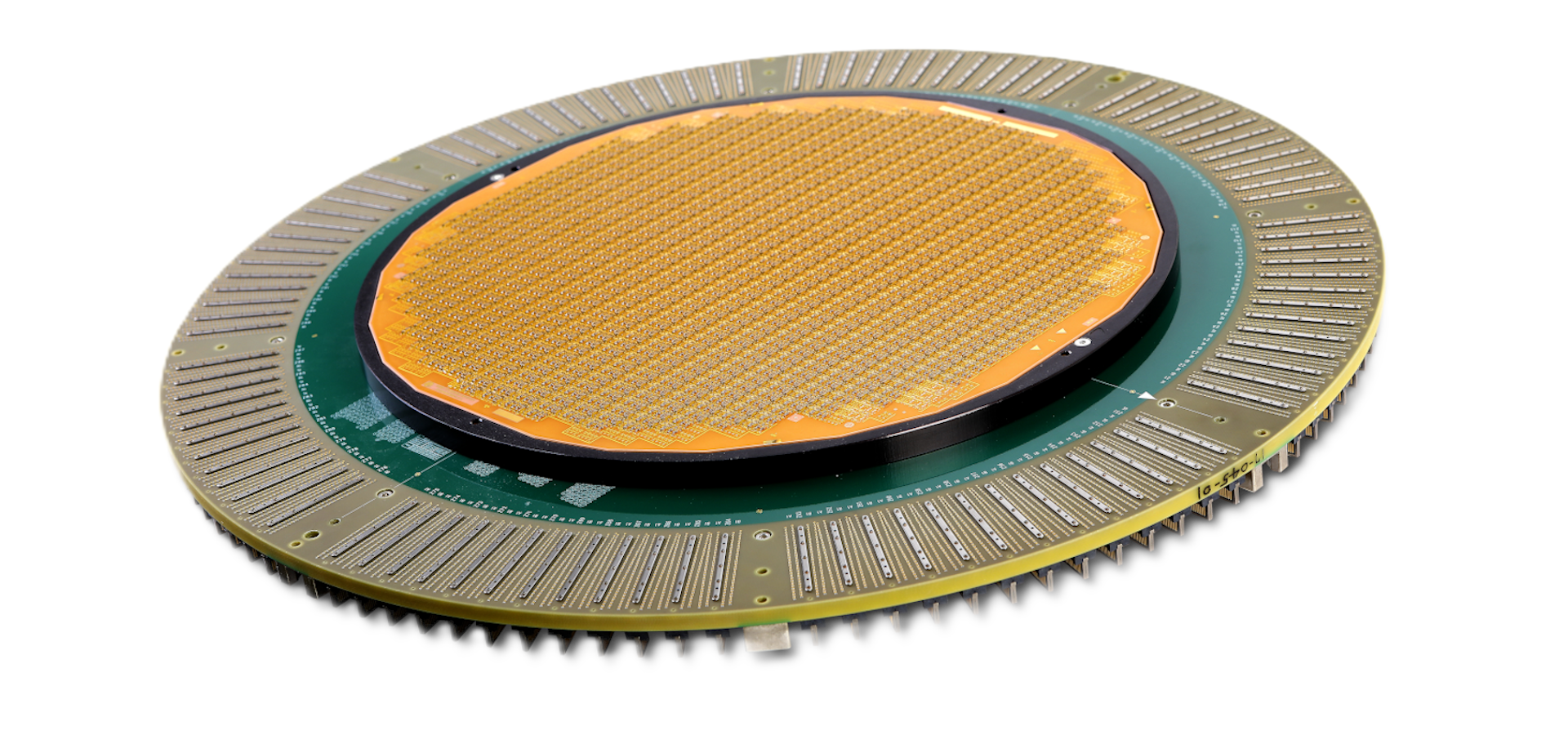
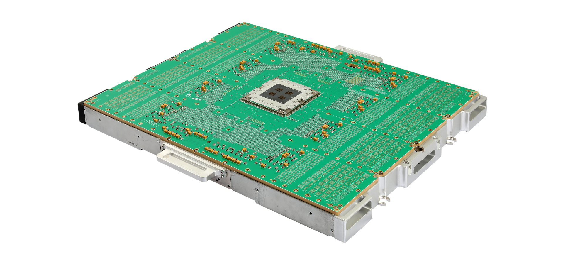
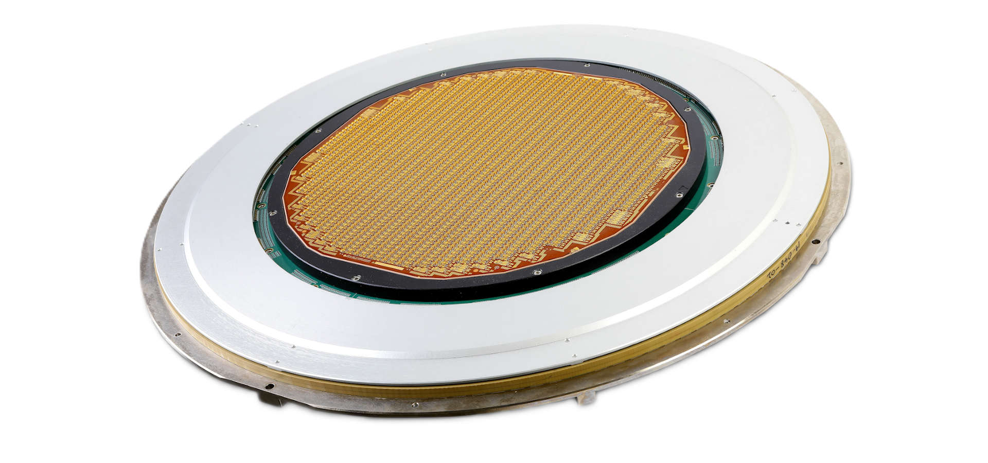 DRAM and HBM MEMS Probe Cards
PreviousNext
Korea Instrument has been a long-standing partner of Samsung. What differentiates your company from competitors in probe card manufacturing?
Our biggest strength is our end-to-end integration. From the initial design stage through simulation, production, fabrication, and final assembly, we manage the entire process internally. This allows us to respond quickly and precisely to customer’s requirements.
We also develop customized equipment exclusively for our use, ensuring we maintain technical independence and efficiency. Our simulation and electrical design capabilities, particularly in signal integrity and power performance, give us a one-to-two-year competitive lead over peers.
Ultimately, what sets us apart is our ability to collaborate closely with clients from conception to delivery, providing consistency, speed, and tailored solutions that others struggle to match.
How does Korea Instrument approach collaboration with global equipment suppliers across Japan or the U.S.?
Collaboration is essential. In bonding equipment, technologies like fine pitch movement, laser power, and precision control must be integrated with probe card design. Without close cooperation, equipment cannot deliver full performance.
From a perspective of test performance verification, currently, we are co-developing high-speed probe cards with one of global test maker, particularly for logic chip test. This kind of joint development is a model we intend to expand, not only with this company but also with other Japanese and American partners when opportunities arise.
In memory, collaboration tends to be more predetermined with Samsung. But in LSI, because requirements are more specialized, joint development with equipment makers is both possible and necessary.
Finally, what is your long-term vision for Korea Instrument?
My vision is for Korea Instrument to become a truly global player in the probe card market. Within the next three to five years, we aim to move beyond our domestic leadership position and establish ourselves as a top-tier supplier in the global probe card market.
We are already making progress: this year we entered DRAM and HBM supply, and in parallel we are preparing for expansion into the LSI sector, particularly in Taiwan and China. DRAM and LSI together will significantly expand our market share.
Diversifying across both memory and LSI not only spreads risk but also strengthens our resilience. I believe this dual strategy is the right approach to ensure stability and long-term growth. Korea Instrument has the history, the technical foundation, and now the strategic ambition to play a central role in the global semiconductor ecosystem.
For more details, explore their website at https://www.kicl.co.kr/
隱私權政策
韓國儀器股份有限公司(以下簡稱「公司」)為了保護信息主體的個人資料,並根據《個人資料保護法》第30條迅速順暢地處理相關投訴,制定並公開如下個人資料處理指南。
第1條 個人資料處理目的
「公司」出於以下目的處理個人資料。所處理的個人資料不會用於以下目的以外的其他用途,若利用目的發生變更,將根據《個人資料保護法》第18條採取獲得單獨同意等必要措施。
甲. 關於「諮詢」的諮詢及回覆
出於處理客戶諮詢、投資諮詢、人才招聘諮詢等目的處理個人資料。
第2條 處理的個人資料項目
「公司」在提供服務所需的最小範圍內收集並利用個人資料。
甲. 無需信息主體同意即可處理的個人資料項目
在互聯網服務使用過程中,可能會自動生成並收集以下個人資料項目。
- IP地址、Cookie、MAC地址、服務使用記錄、訪問記錄、不良使用記錄等
乙. 經信息主體同意處理的個人資料項目
「公司」根據《個人資料保護法》第15條第1款第1項及第22條第1款第7項,在獲得信息主體同意後處理以下個人資料項目。
- 客戶支援諮詢:收集項目:姓名、電子郵件、聯絡方式
第3條 個人資料的處理及保存期限
「公司」在法令規定的個人資料保存·利用期限或收集個人資料時獲得信息主體同意的個人資料保存·利用期限內處理並保存個人資料。
各項個人資料的處理及保存期限如下:
客戶支援諮詢:永久(收到刪除請求時立即刪除)
但是,若符合以下事由,則保留至該事由結束為止:
因違反相關法令正在進行調查、偵查的情況:至該調查、偵查結束為止
因使用網站而殘留債權、債務關係的情況:至相關債權、債務關係結算完畢為止
第4條 個人資料的銷毀程序及方法
個人資料在保存期限屆滿、處理目的達成等個人資料變得不再必要時,將延遲銷毀相關個人資料。
儘管從信息主體處獲得的個人資料保存期限已過或處理目的已達成,但根據其他法令仍需繼續保存個人資料時,將該個人資料(或個人資料文件)轉移到單獨的數據庫(DB)或更改存放場所進行保存。
個人資料銷毀的程序及方法如下:
銷毀程序
「公司」針對需銷毀的個人資料(或個人資料文件)制定銷毀計劃並進行銷毀。「公司」選定發生銷毀理由的個人資料(或個人資料文件),經公司個人資料保護負責人的批准後銷毀個人資料(或個人資料文件)。
銷毀方法
「公司」對以電子文件形式記錄、存儲的個人資料,採用低級格式化(Low Level Format)等方法使其無法恢復記錄;對記錄、存儲在紙質文檔上的個人資料,則使用碎紙機粉碎或通過焚燒銷毀。
第5條 個人資料安全性確保措施
「公司」為了確保個人資料的安全性,正在採取以下措施:
管理措施: 制定及實施內部管理計劃、定期員工培訓
技術措施: 個人資料處理系統等的訪問權限管理、安裝訪問控制系統、安裝及更新安全程序
第6條 關於自動個人資料收集裝置的安裝、營運及拒絕的事項
< 自動個人資料收集裝置安裝及營運 > 「公司」為了向用戶提供個性化的定制服務,會使用存儲並隨時調用使用信息的「Cookie」。
Cookie是營運網站的服務器(http)向用戶電腦瀏覽器發送的少量信息,有時也會存儲在用戶PC電腦的硬碟中。
信息主體可以通過Web瀏覽器選項設置來允許或阻止Cookie。但是,如果拒絕存儲Cookie,可能會在使用定制服務時遇到困難。
Web瀏覽器中的允許/阻止Cookie設置
- Chrome: 瀏覽器設置 > 隱私和安全 > 清除瀏覽數據
- Edge: 瀏覽器設置 > Cookie 和網站權限 > 管理和刪除 Cookie 及網站數據
移動瀏覽器中的允許/阻止Cookie設置
- Chrome: 移動瀏覽器設置 > 隱私和安全 > 清除瀏覽數據
- Safari: 移動設備設置 > Safari > 高級 > 阻止所有 Cookie
- Samsung Internet: 移動瀏覽器設置 > 瀏覽歷史 > 清除瀏覽數據
第7條 個人資料保護負責人
「公司」全面負責個人資料處理業務,為處理與個人資料處理相關的信息主體投訴及損失救濟等,指定個人資料保護負責人如下:
▶ 個人資料保護擔當部門
部門名稱: 人事團隊 (HR Team)
聯絡方式: +82-31-375-5900
電子郵件: ki.hr@kicl.co.kr
信息主體在利用「公司」的服務(或業務)過程中發生的所有個人資料保護相關諮詢、投訴處理、損失救濟等事項,均可諮詢個人資料保護負責人及擔當部門。「公司」將對信息主體的諮詢及時給予答覆和處理。
第8條 個人資料處理方針變更
本個人資料處理方針自2025年09月01日起施行。